Summary
This is a snapshot of a rather accidental project and is presented in a chronological order from inception to hitting an initial milestone. A broad range of topics are covered ranging from digital audio, digital video, a wireless data link, a small embedded USB host, generation of graphics and text on-the-fly, power supply analysis, mechanical construction, to name but a few topics. The project is designed around a low cost FPGA engine, and also includes creation and programming of a soft-core 32 bit microprocessor.
This is also not intended to compete with the newer generation of Linux-on-a-card systems. One of the overriding philosophies here is less-is-more with much more attention to detail down to the absolute lowest levels of the system - whether it be special hardware, or custom software. The project was also implemented at absolute lowest cost, with the intent of maximum education.
This is not intended as a construction project, but there may be techniques and ideas presented that may encorage experimentation, or at least spark of enough interest to cause some dark technology corner to be explored that has been previous ignored.
Mark Atherton, August 2013, New Zealand.
Background
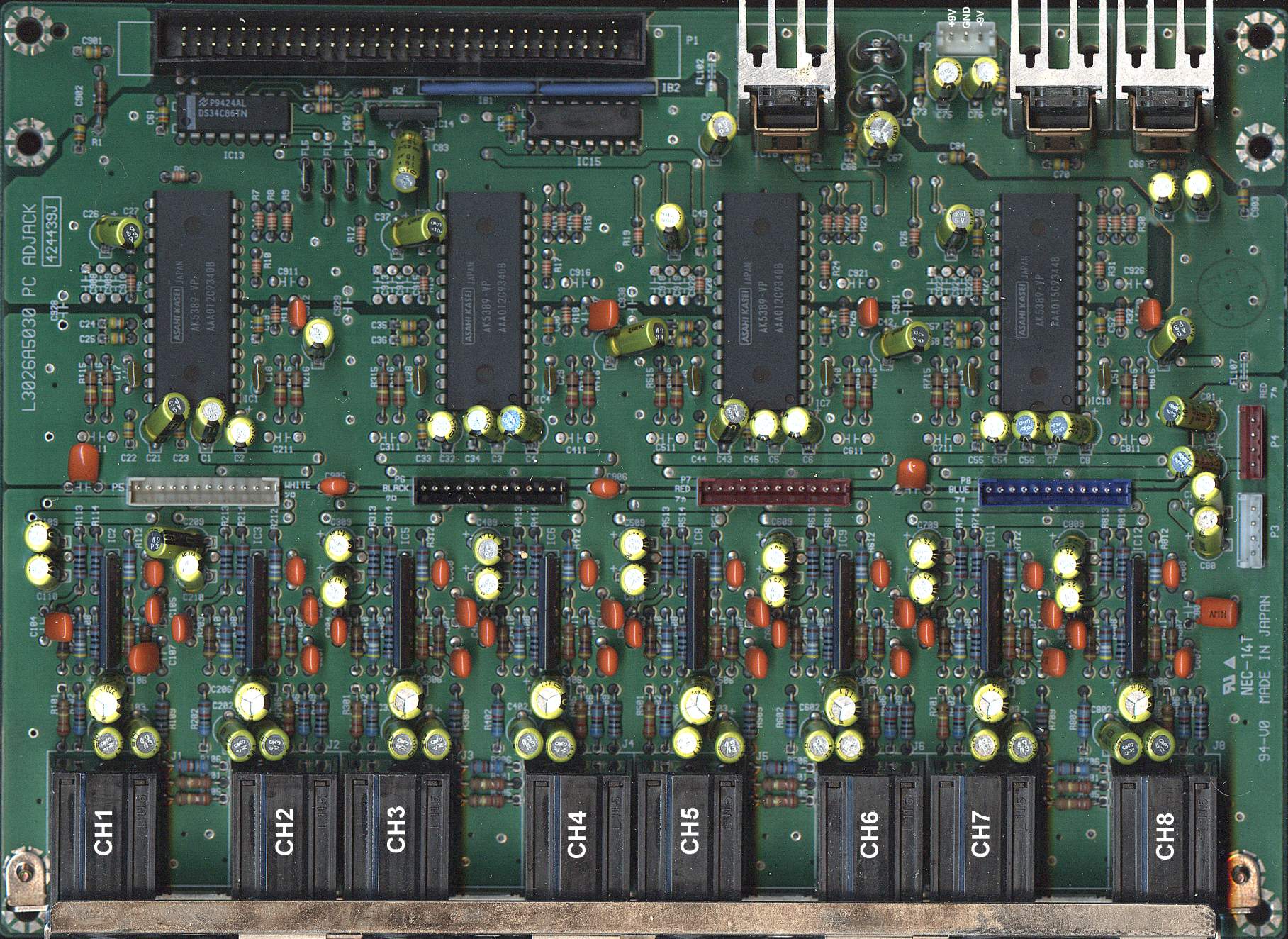
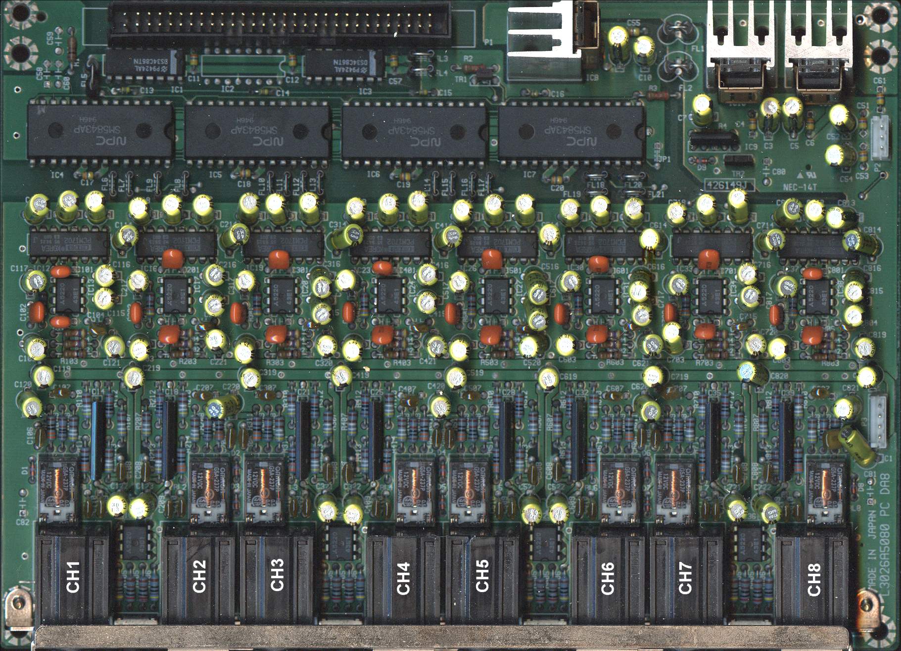
Minding my own business one day while down at the scrap yard, I tripped over a rather sad and rusty steel box-of-knobs. Further investigation revealed that it was actually an Akai DR8 studio hard drive recorder that has masses of stuff missing, but apparently all of the analogue input (ADC) and output (DAC) cards were intact. So each card was carefully unbolted and inspected for physical damage - of which there appeared to be none. So the cards were brought home, thoroughly washed, dried and a search done to find out more about the swag.
Between the web, and a datasheet search, the card-set appeared to be as follows:
Repair and Testing
Before too much time is spent dreaming about possible uses, some effort should be put into board repair and performance evaluation.
Between board markings and component data, it was reasonably easy to figure out that the boards ran on +-5V and +-12V. A couple of 78 series regulators were busted and straightforward to replace. Correct voltages then appeared as expected.
So power is now OK, but some form of verification is required that the digital and analogue signal paths are all OK. From the datasheet, it appeared that all DAC oversample filters and ADCs were configured for serial data (much like I2S), but with L/R changing state one clock cycle early. Data should be presented MSB first.
A CPLD test board was to hand with an EPM7128 loaded. This part has 128 Complex Logic Block elements, and can be considered to be a small FPGA. A 48 step 1kHz and 2kHz 18 bit sinewave was synthesized using some quick-and-dirty C, and loaded into a Verilog lookup table. There was then just enough room left to add required clocking to allow the board to generate 256Fs, BC, LRCK and DATA as required by the DAC boards. It didn't take too much more effort to persuade each of the DAC channels to create a full scale analogue sinewave.
With the DACs working, the CPLD test unit could then be used to clock data between the ADC and DAC boards (given that each used the same serial data format). With back-to-back testing and some help from a PC based audio test unit (Audio TestSet V2) all ADC channels appeared to work just fine.
During the testing-and-poking-around phase of the project, notes were also made about the multi-pin interconnect which would later form the basis for an small interface PCB.
Finally, it was possible to make a reasonable estimate of total power supply burden based on individual card measurements.
In any case, this has been remarkably lucky find.
Project goals and Architecture
I have had a life-long interest in audio, and was even lucky enough to work for a small outfit in the US for some considerable time who did such things. So this card set provides quite an opportunity to build a box of [digital] audio bits to experiment with.
Having a collection of boards spread around the bench with masses of wires is a sure way to cause frustration at many levels. So some kind of mechanical frame, power supply, power distribution and processor platform is quite desirable.
A flexible processing platform is also desirable, so that different architectures can be explored as required.
There should also be a reasonable amount of spare space so that peripherals can be bolted on around the processor. Not sure what or how at the start of the project, just didn't want to start off too crowded.
Mechanical
Desirable attributes of the frame:

Main frame was made from 1.2mm ali that had been cut and folded at a friends workshop. All material was cleaned using an orbital sander and de-greased prior to assembly. The finish is a bit industrial, but "It's a box to tinker with, not a product", as noted above.
Toroidal power transformers were bolted to the end cheeks. Associated external bolt heads were made flush with the aid of a homemade dimple-maker. Boards were stacked using M3 F-F and M-F brass hex standoffs along with some custom standoffs and stud made in a lathe. Handles were made from 10mm hex stock, drilled and tapped to M3. Most parts were made to drawings rather than cut, locate and drill. This enables alternate processor plates etc. to be made with minimum fuss in the future.
The expense of the ali has been rewarded by a very cool running unit (chassis used as a heatsink), by virtue of the very low thermal resistance of the material. The unit is also quite light, with the transformers being the heaviest components.
Processing Engine
An FPGA offers almost infinite possibilities for these kinds of projects since they can be configured to provide (for example) a serial interface to fetch data from an ADC or send data to a DAC. A convolution engine can be built as part of an audio equalizer, and a 'soft processor' can be built to provide some form of user interface.
The DE0-nano is a lovely small, low cost FPGA development board manufactured by terasIC and is supported by the Altera (free) Quartus II development software.. This module has as it's heart an Altera Cyclone IV EP4CE22F17C6N device with about 22,500 Logic Elements (quarter of a million traditional gates (?). The module also has a 16MB config device, 32MB of SDRAM, a plentiful supply of user I/O, along with an embedded USB-blaster programmer and a on-board 50MHz system clock.
Quartus II, Schematics, Verilog and NIOS II
Traditional digital hardware design is usually done by the creation and analysis of a schematic. Quartus II (QII) allows shematic entry as well as textual entry using either Verilog or VHDL. Verilog looks the least daunting of the two HDLs from the point of view of an old and crusty C programmer since it shares a very similar syntax.
The web edition of QII is free, and while it doesn't have all of the bells and whistles of the $8k(?) versions, it is quite a bit less expensive. The main features missing are IP cores (pre-compiled technology blocks), and optimization that allows compilation using a multi-core host CPU. Despite the limitations of the free version, it still has a capable set of features including a mega-wizard that allows the creation and customization of some interesting blocks including dual port RAM with different data widths on each side, and a soft CPU core generator.
QII is supplied with a complete set of tools to manage the creation of a 32 bit CPU, again by the use of a wizard. This allows quite interesting custom core+peripheral sets to be built easily. Supplied peripherals include the usual UART, SPI, GPIO devices, interrupts - each of which can be instantaniated as many times as hardware resources allow. Not perhaps the most grunty engine on the planet, but at 50MHz it can manage some half reasonable processing.
The free version of QII does not allow the inclusion of a cache but (I believe) floating point hardware can be compiled in at the expense of additional logic resources. One other interesting feature is the ability to built a multi-processor (not just multi-core) array, with inter-processor shared memory semaphore, FIFO or postbox communications.
A tightly integrated C toolchain is also included which allows a Board Support Package to be easily generated for each configuration. Compiled code can run out of either on-FPGA RAM (78k in the case of the DE0-nano), or the 32MB of supplied off-FPGA SDRAM.
Finally, the DE0-nano has a built in JTAG programmer which talks directly to QII, so this is quite a well integrated package-set.
FPGA to real world interfaces
A small interface PCB needed to be made to connect the FPGA board to the balanced signals on the 60 way ribbon which connected all of the ADC and DAC boards together. While electrically simple, this took a monumental amount of gate-swapping to reduce routing complexity. This can be seen as a paper template in the basic frame photo above.
An async channel was provided through the use of a modified serial-USB mobile-phone data cable. This would be the inital comms channel to command the soft processor on the FPGA via a simple Command Line Interface (CLI). In the latter parts of the project, this interface would move to a small piece of stripboard and mechanically share space with the SPI wireless interface.
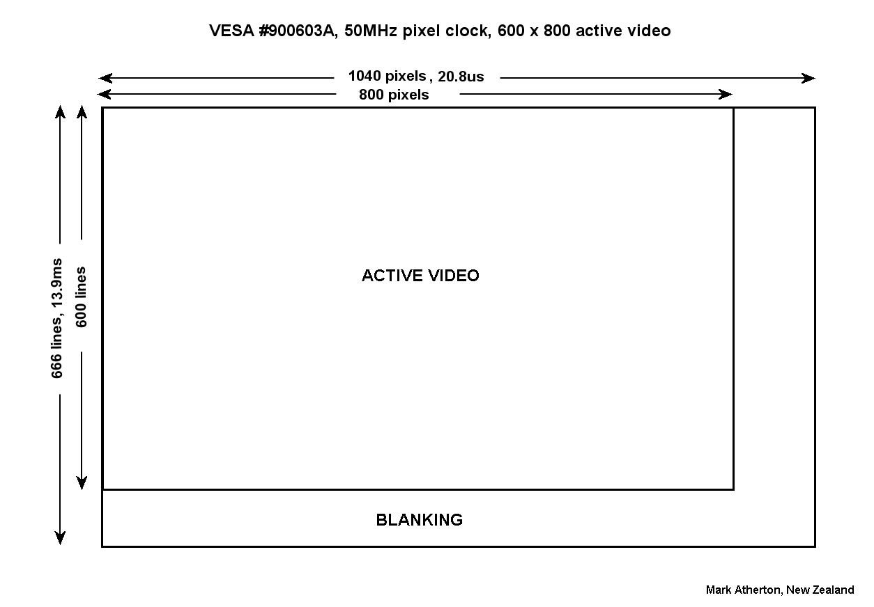
A High Density 15 way connector allowed a VGA monitor to be attached via a video DAC. There was a surprising amount of work involved in the design and fabrication of this tiny board. Issues included wiring complexity vs video resolution (2:2:2 was chosen with help from here). Also the unit had to provide level translation between 3V3 signaling from the FPGA while maintaining better than 20dB return loss over DC-100MHz while feeding 75 ohm VGA coax. A resolution of 800 x 600 at 72Hz was chosen from the VESA standards (VESA #900603A) since this would provide a usable User Interface on a physically small display. Timing for this standard could also be conveniently derived from the on-board 50MHz clock.
Last but by no means least is the matter of power distribution. The unit requires regulated +-12V (line inputs and line output opamps), unregulated +-9V (ADCs, DAC, DAC filters), and +5V (FPGA, Wireless and Video). It would be so easy with this kind of a project to wire all of the power point-to-point but an extra few hours was spent making a multi-pin distribution board using stripboard and 8 pin connectors. A ground was brought out for each of the three rails so that the PCB assemblies could be used as the correct analogue/digital ground connection point. No earth loops have been observed so far.
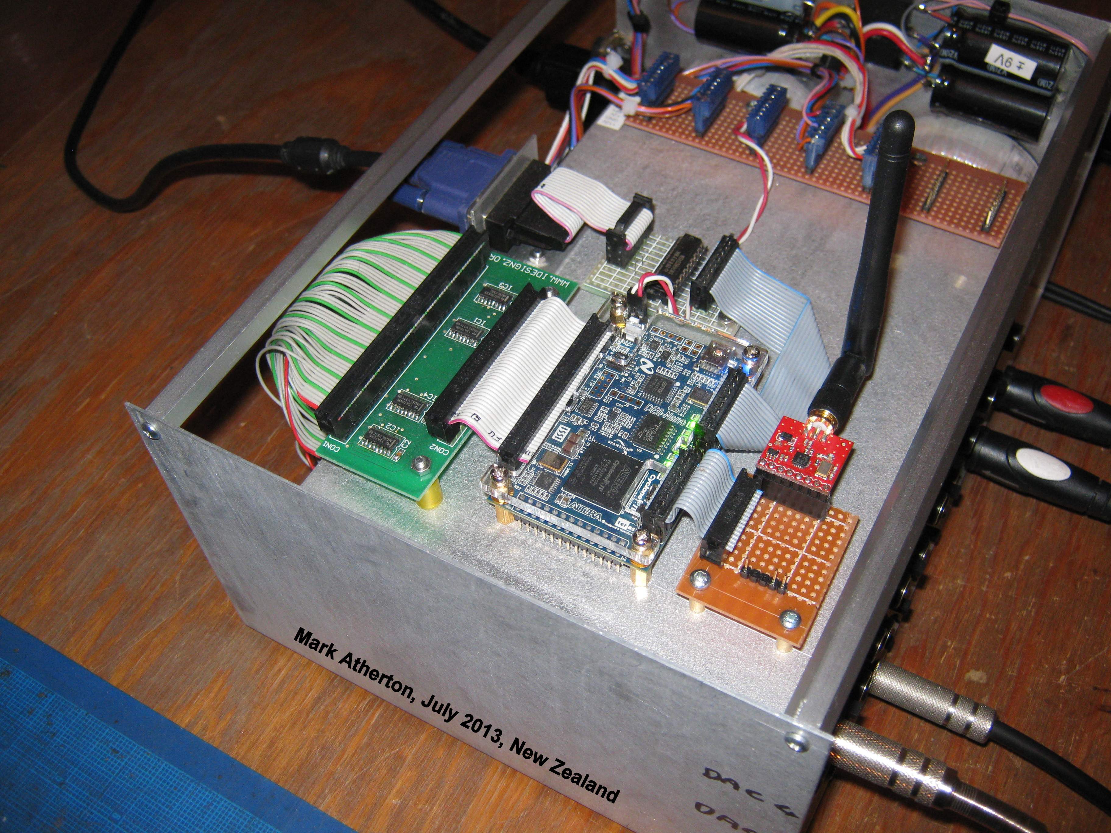
The green PCB to the left of the DE0-nano with the 60 way ribbon cable is the differential interface to the digital audio boards. The board above with the DIP part is the VGA interface with 3 x 2 bit DACs driving RGB. The board to the right connects to the nRF24L01A+ wireless interface (SPI) as well as a three pin header for the UART. At the top, the DC power distribution board can be seen. This has 7 connectors, each with 8 pins and separated grounds.
First experiments: NIOS II and the audio matrix
One of the first questions to be investigated was 'just how useful are 22,500 logic elements' for real world applications. An obvious first activity was therefore to build DAC and ADC interfaces which convert the (nearly I2S) serial data streams into 18 bit parallel data. A single master clock generator provides 256Fs, BCLK amd LRCLK timing while shift registers and appropriate logic shift in and shift out data for this interface. These three basic units were written in about 114 lines of commented Verliog. One of the delights of this development method is that once a building block has been designed, re-use is trivial.
In terms of the switching matrix inputs, four fixed frequency oscillators were built using a DDS technique (more about that later). This in addition to the 8 analog inputs formed the twelve input sources. The 8-output-DAC-boards were used as the data sinks. Each DAC input was fed from a twelve input multiplexer. Bear in mind that all of the switching fabric is 18 bit wide parallel data.
A small processor was also required to control this whole mess, so one was built using the NIOS II system builder (SOPC). User I/O was at 9600 baud over an async channel. User input was then translated into a single 32 bit word which controlled audio selection of 8 of the DAC. The remaining 4 DACs were fed with test tones.
For inital simplicity, the chosen design method was to use schematic capture to connect verilog modules together. Here is the design of the finished test unit. Building and testing each piece of the puzzle before system integration resulted in a well behaved and predictable system. As well as experimenting with new design methods, this was also a test of 'usefulness' of the FPGA. So routing fabric was 18 bits wide, and the full matrix was 12 x 8, so this is 18 * 12 * 8 = 1728 'wires'. Add to this the complexity of a 32 bit soft processor and associated compiled C.
Device usage
So a very simple audio switch has been built, some order-of-magnitude measurements have been made to allow the relative usefulness of the DE0-nano FPGA board to be estimated. Also, a toe has been dipped into the generation and programming of soft-core processors.
Test Signal(s)
A programmable fixed frequency, fixed level oscillator allows first-level testing of new components as they are developed. Add an audio gate and a simple tone burst generator can be built. Use two generators, with frequency set 1Hz apart and the 1 second cycle time of the mixing product can be used for linear amplitude sweeping.
In it's simplest form, a 256 step * 18 bit lookup table can be used as the data source. With a 50MHz master clock divided by 1024, audio sample rate is 48,828Hz, so fetching one table entry per sample clock would produce a sinewave of just over 190Hz.
Instead of using an 8 bit (256 step) counter to index the data from the table, use a 24 bit register, where the top 8 bits form the index and the entire 24 bits allow for fixed-point addition in an unsigned 8.16 format. So if integer steps through the table yield a 190Hz tone, this new variable allows an increase in frequency resolution of 1 in 2^16, or 190Hz/65536, which is about 3 milli-Hz. This is a similar order of magnitude as the frequency accuracy of the crystal timebase, so is a reasonable lower limit. Since there are 8 bits to the left hand side of the decimal point, this allows the possibility of indexing data which is higher than sampling theorem permits, so is also a reasonable limit. So now with this 24 bit phase accumulator allows the generation of test tones in the range 3 milli Hz to 24kHz in 3 milli Hz steps.
For the audio matrix test, four test tone generators were setup at 1000.0Hz, 2000.0Hz, 4000.0Hz and 8000.0Hz - with direct connection to 4 of the DAC outputs. For later tests, one osc was set to 1000.0Hz and second to 1001.0Hz allowing a 1Hz beating product to allow amplitude sweeping of modules under test.
The 8 into 2 audio mixer
The next step in the project was to create a simple audio mixer that can take eight analogue inputs and mix them into a stereo output. Each input will be metered, will have a level control slider and a balance pot. The control surface should be available off-the-shelf, and should connect to the audio box via wireless. Each input signal should be displayed dB accurate on a bargraph, along with a suitable PPM hold and decay mechanism.
Video
Traditional video sub-systems (within PCs etc) use a frame buffer to hold an image. As a gross simplification, this is dual port (DP) RAM that has boxes, text, graphics etc. rendered either directly by software (from the CPU), or indirectly by a Graphics Engine (GPU). The RAM is then sequentially read by a counter and the contents of each location is passed through a DAC before being sent to the display. For our application, there really isn't enough DP RAM on the FPGA to create video in this manner, however there is quite an abundance of configurable hardware resources.
The Raster
For the chosen resolution of 600 x 800 pixels, VESA #900603A indicates that the master pixel clock is 50MHz, that there are 1040 pixels per line (800 active), and 666 lines per frame (600 active). So line rate is 50MHz/1040 = 48.077kHz, frame rate is 72.19Hz, and scan is progressive. This standard also specifies in detail timing and placement associated with horizontal and vertical sync. It is also worth noting that of the (1040 x 666) 692,640 scan pixels, only (600 * 800) 480,000 are usable, the unused pixels fall within video blanking. All manner of interesting things happen if you generate video during this non-display (video blanking) time...
On The Fly Graphics
The audio mixer graphical user interface (GUI), as with most GUIs, needs to be assembled from a collection of atomic building blocks. In this particular application the following might be quite useful:
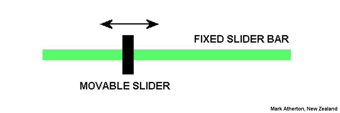
The display comprises three layers: foreground, context and background. Foreground is the item that can move under the control of stimulus, such as a slider. Context is a border or a rail, which provides the visual cues, required to give the movable entity context. Background is the static rendered video that is displayed when neither foreground nor context is being generated.
In the case of a horizontal slider, this has a movable black rectangle which is drawn first, and below it a green slider bar.
Similar rules apply to the generation of the black slider, but in this case pixel_counter is compared against a register whose value can change (and defines movement). In this case, line_counter is still compared against fixed values since the graphic entity is not allowed to move vertically.
A further level of sophistication is possible when the values of the register which is used to set position are also used to modify the colour of the entity being displayed. This is the basis of an audio bargraph where signal level affects colour - RED being high level, YELLOW being mid level and GREEN being low level. In this case the context layer would be rendered as a grey outline that encases all possible bargraph movement.
On The Fly Text
Some form of textual output on the display allows for screen annotation as well as status updates from the processor. The two classes selected for this project were:
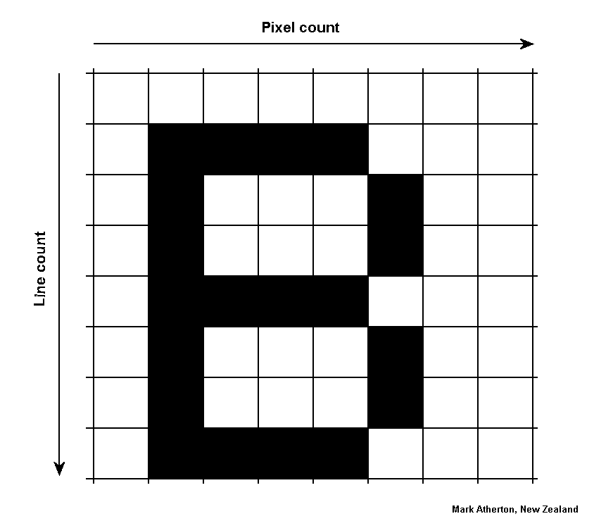
The FPGA provides 600k+ bits of on-chip-memory, which can be arranged into many different types of architecture with the help of a very tightly integrated, and easy to use mega-wizard (MW). The Character Generator ROM was built as a single port 8*8*7 structure (128 characters, arranged 8*8) and required 8192 bits of initialised memory. The contents of this memory block were pulled out of a rather old RO2513 with help from an olde-worlde Dataman S4 EPROM programmer.
Since it is possible to synthesise different width ROMs using QII, a significant simplification of the character video system occured by the use of a 1 bit wide ROM, rather than the traditional use of an 8 bit wide ROM and associated 8 bit shift register. So the 8192 bits of the CG ROM were arranged: A0..2 pixel count, A3..5 line count, and A6..12 character selector.
Since the screen is organised 800*600 pixels, from an 8*8 CG ROM, this would allow for text to be displayed 100x75 characters. This is too high resolution for background text in this application, so it was decided to repeat every pixel and reduce resolution to 50*37 characters.
This does not readily fit in the digital 2^n world, so the final RAM size was arranged 64*32. For the sake of hardware simplicity, 14 characters are lost per line, and reading of the text RAM is delayed by about 2 characters to allow 32 lines to be displayed where 37 are required. So the final requirements for this Dual Port RAM was 64*32*8 = 16384 bits/2048 bytes per port. A burden on the generation of this memory block was to select and option that keeps the read side of the RAM intact should a conflict occur while the CPU is writing to the memory; this was chosen to avoid the text from flickering during message updates from the CPU.
The console sub-system was intended to be used for debug, so quantity of information was more important than readability. This design was similar to the background-text sub-system with a few important differences:
Hardware scrolling was surprisingly simple, and was implemented using a well balanced mix of hardware and software. A 256 byte dual port memory was constructed, with each location holding an ASCII character. Character memory on the write side is accessed using the NIOS II processor, while on the read side, data is fetched using hardware in conjunction with an 3 bit register which is shifted 5 places and added to read pointer; this allows hardware scolling, one line at a time. Console display position can be set using a pair of X/Y registers and there is a console display/hide bit.
NIOS II, cont'd
As has been mentioned earlier, QII has a tightly integrated system builder wizard which allows quite complex microprocessor cores(s) to readily be constructed. The workflow basically involves dragging and dropping various components into a form that then allows address, data and interrupts to be connected as required. Next, address ranges need to be assigned to each entity, so they are uniquely accessible. This is followed by 'generate system' which synthesises HDL in the chosen language (Verilog or VHDL). Finally, a symbol, or HDL prototype is available a the highest level for system integration. In firmware-land, a Board Support Package (BSP) needs to be generated (within the associated Eclipse IDE). These system headers then allow the firmware to communicate with the new hardware.
It is also possible to construct custom interfaces, so specialised components can be communicated with. This is all fine as long as the designer has fully established the required interface, which is not so in the case of this project since it is so thoroughly experimental. Another method needed to be developed that would allow I/O to be developed rapidly without incurring the time penalty of the whole workflow.
By bringing the CPU bus interface through a simple portal, external memory mapped devices can be attached and debugged as required. This does add slightly to the level of comlexity in terms of having two distinct address spaces, but the advantages brought about by this type of architectural decoupling has more than made up for it.
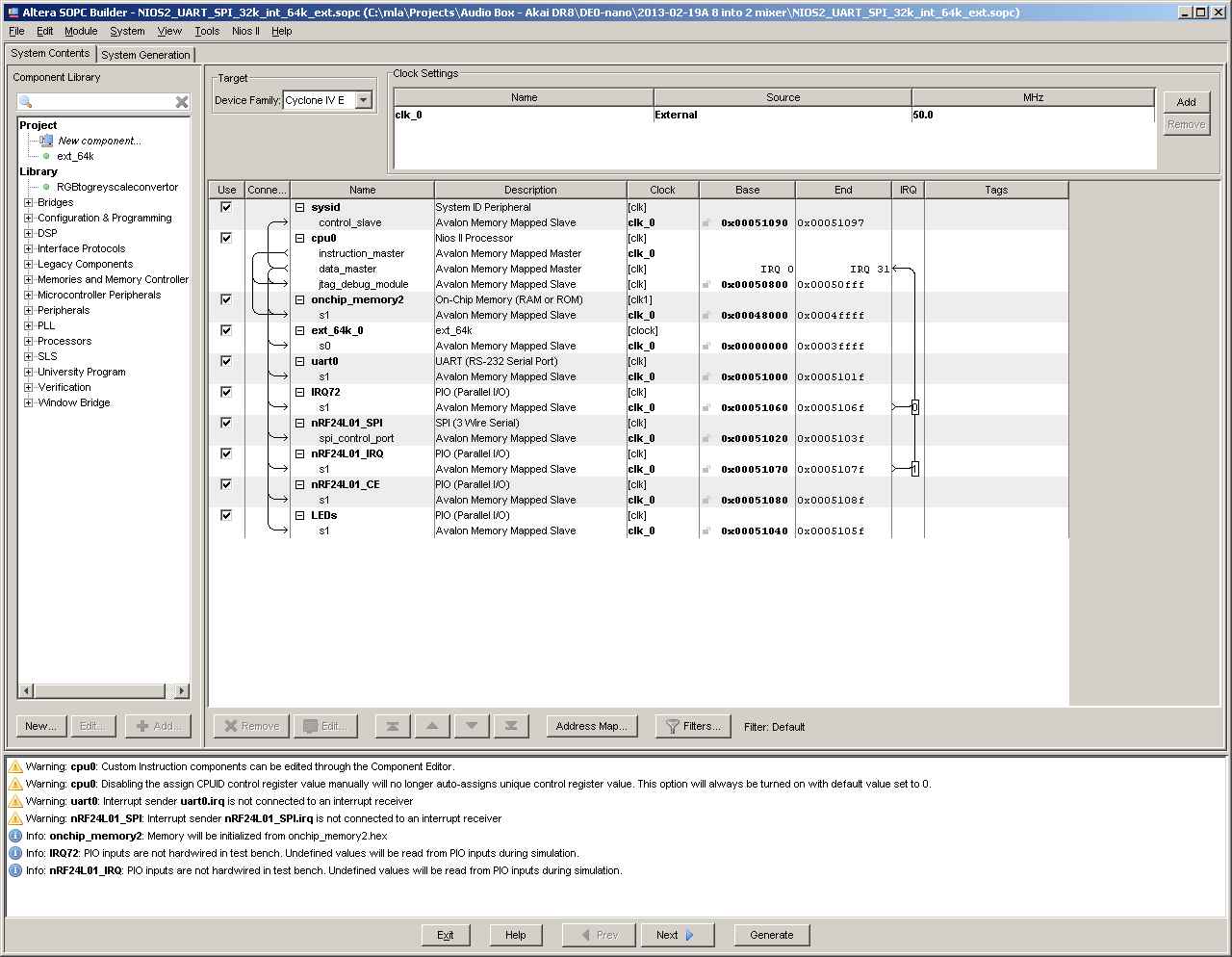
Notice ext_64k_0, this is a memory portal 64k * 32 on the CPU side of which the lower 8 bits are carried through to the external interface. While this is not a memory efficient interface, it does reduce complexity of required logic as well as less confusing memory interface firmware.
Summary of CPU and associated components
The external memory map was defined quite early in the project and was (obviously) quite indispensable for sub-system design as well as test. Notice that several modules have block select address lines (S0..3), allowing multiple instances of the same module to be used, and allowing unique access.
Data Conversion : PPM and dB conversion
So far we have building blocks that can provide PCM audio as signed 18 bit quantities; data sources so far include ADCs, tone generators, and tone burst gates. We also have the means to render bar graphs in real time; the most natural data range to control these entities is a small unsigned value with a data range larger than the number of pixels to be rendered.
Two processes are required to convert the PCM audio before it is suitable for presentation. The first is the PPM unit (Peak Programme Meter), and the second is a means to convert this (now) unsigned 17 bit quantity from linear to log - but extremely fast.
PPM. So this module need to rectify (take an absolute value) the incoming PCM, then hold the highest value. At a predetermined rate, a logrithmic decay now needs to be applied so that peak values are only held for short periods before they drop away. This latter feature was implemented by using a (72Hz) timer to trigger a mechanism which multiplies the current value by a fixed fraction. The result of this process is still in U17 format, so requires further work before it may be displayed.
dB conversion. The ear has a logarithmic sensitivity to level change, with 1dB being the smallest perceivable difference, also given that the vertical bargraphs are going to be 256 pixels high, natural scaling occurs if we can accept 0..-63.5 as this represented range. Using a simple FLOAT library with the NIOS II processor running at 50MHz, initial attempts at logs resulted in a few conversions per second - this could have been significantly faster if the floating point engine had also been used. In any case, even if this approach could have been made to work at the required video frame rate (72Hz) there would have been little remaining CPU horsepower available for other tasks.
Fast Approximation. Time to optimise, and investigate a possible hardware only solution. Requirements can be trimmed back quite a bit if the output only needs to be 128 half-dB steps (0..-63.5dB), with a requirement that the conversion is monotonic with no missing codes. A few things are apparent peering at linear level vs digital value, the most obvious is that one bit position of data movement changes signal level by 6dB (actually 20log(2/1) = 6.02dB). So if the incoming data can be shifted until there is a zero in the MSB of the shift register, and a 1 at MSB-1. Every time we do a shift, we add -6dB to our result. With this shift and count complete, we can now look at the remaining bits located in bit positions MSB-0 through MSB-7. A spreadsheet was constructed that took a ratio of 1.0 as 0dB with 7 bits precision and calculated 11 more steps in -0.5dB increments. By comparing the 8 bit value located MSB-0 through MSB-7 against this table, the precision of the calculation could be increased to 0.5dB per step.
A simulator was written in C to confirm that all of these ideas worked, then a state machine was build in Verilog which executed the same process at 50MHz. The result was a machine that could manage over 1.3 million PCM -> dB conversions per second, which is not too bad. The downside of this machine was the hardware burden of about 300 logic elements per instance. A compromise was reached and the C simulation code was compiled as a fixed point calculation for the NIOS II processor and final execuation time measured at 7us per conversion. Finally, the 72Hz video frame interrupt was used to call this conversion routine, and the ten conversions (one per bargraph) were executes sequentially.
Audio gain control, mixing and limiting
For an eight input, two output mixer, each input channel needs some form of gain control, a method of summation, and a clean method of clipping before passing the data to the output channel. The simplest way to describe the input audio is a signed 18 bit quantity, so this will be referred as an S18 from now on. The control path for level setting was initially a U16, but Verilog has some less-than-obvious rules about type casting if you wish to synthesise S18 * U16. To save associated complexities and confusion, gain was managed by S18 * S18.
At each output summation point, there is the possibility that eight full scale input signals could occur simultaneously. Clearly this could be a source of gross overload and distortion. Another possibility is divide each input channel by eight before summation - this would result in about 18dB of dynamic range for the system. The chosen method was to accumulate the result to an S22, so there were several spare bits at the top end available to accommodate overload, so S22 out_PCM = ((S18 ch1_PCM * S18 ch1_gain) + (S18 ch2_PCM * S18 ch2_gain) ... ). After accumulation, the top four bits should all be the same (4'b1111 of 4'b0000) if overload has not occurred. If this is true, then the lower 18 bits of the accumulator can be used as-is. If this test is false then B21 of the accumulator is used to decide if + or - full scale should be used as the output value.
A final level of complexity was the pan control. If channel 1 pan is moved to 'pan right 6dB', system complexity is lower and full dynamic range maintained if the left output is dropped 6dB etc. The converse also being true.
Final hardware and software architecture
At this point all of the major hardware building blocks required to build the mixer have beed discussed (apart from wireless control which will be covered later). The system is very much a case of software-assisted-hardware.
The main display update thread is executed within an interrupt running at video frame rate (72Hz) and is responsible for fetching rectified data from the Audio Peak Program Meter (PPM) engine, converting this linear data into dB (which takes 7us), then updating the VU display engine. The wireless interface is interrupt driven as data becomes available from the USB control surface. This routine is also responsible for converting mix and pan levels into audio control values which executes in a few microseconds. That is basically all that is required to manage the hardware.
Main area requiring improvement is the current use of 8*8 character generator which renders as rather a retro font - need to see if a 16*16 is available. The fixed (rather than proportional) font spacing allows for extremely simple hardware design.
Wireless Control Surface
No one but the Die-Hard-Dilbert (DHD) would consider using the command-line-interface to control the mixer, so some form of physical interface was required. With the advent of the Digital Audio Workstation (DAW), a whole new class of PC peripheral has been formed - the uncommitted control surface (CS), with manufacturers including Korg, Mackie, Digidesign and Roland. One extra feature that would be nice is the ability to make the control surface wireless.
Summary of requirements
MIDI-over-USB
Quite a bit of work and investigation is required before this stand-alone unit could form part of an integrated wireless unit. One of the first tasks was to get the unit working with a desktop to understand the command syntax of MIDI over USB. All that was required was the ability to change indicator states and read changes of slider and knob movement on the CS. This was a surprisingly easy task using the MIDI_MAPPER supplied as part of the VC6 runtime, running on XP. A similar test was made using Linux, where the device appeared as /dev/midix, so was very easy to read from and write to.
Earlier investigations using USB in and embedded environment were quite sufficient to persuade me that a pre-built library was the way to go with this project. Given that an embedded USB host was also required, this added even more complexity to the task. Embedded processor selection was based almost entirely around availability of appropriate USB host code, cost of toolchain, and community support. After some work the Microchip dsPIC33EP256MU806 was chosen. This part supports OTG USB, so has a USB host as well USB device, and for an un-related project also supports Motor Control. Finally, the part was available mounted on a uJET32 development board from eBay for around US$30. A PICkit3 programmer had to also be purchased, and a decision was made that it was time to migrate from the older MPLAB 8.5 IDE to the new MPLAB X development environment. The "Microchip Solutions v2012-10-15" application library comes complete with "Host - Audio - MIDI" example code, and again, it wasn't an enormous amount of work to translate MIDI-over-USB to/from MIDI-over-ASYNC at 57.6k baud in hex.
Wireless Data
Next major decision revolved around wireless interface. About 20M range seemed reasonable for indoor use, and the more work the part could do, and the more highly integrated the part was, the better. It didn't take too much effort to decide that the NordicSemiconductors nRF24L01+ would be a likely candidate since it appeared to be a complete data radio as well as containing a hardware based communications stack. As a final bonus, there were several suppliers of this tiny (4x4mm) part mounted on a PCB along with RF interface (RP SMA), required 16MHz clock, and digital (SPI) interface brought out on a 0.1" pitch connector. After some investigation the Sparkfun WRL-00705 was chosen, which at US$20 is not the cheapest on the market, but promised to be the best assembled.
A pair of uJET32 boards with dsPICs mounted have been bought for the USB Host part of this project and it seemed prudent to complete the data link using these board then migrate the resulting code for the receive end over to the NIOS II processor when the drivers had been completed. This did result in some duplication of effort, but saved having to haul the audio-box around unnecessarily.
The comms protocol associated with the nRF24L01+ is called Enhanced ShockBurst and is capable of automatically managing quite a well protected data link. After the part has been configured, payload data is loaded into one of the TX FIFOs, TX_EN is asserted for 10us (using a timer) and the TX_ready bit is set. Transmission of preamble, address, packet control field, payload and CRC is then automatic. If the PRX end fails to acknowledge within a preset time then a retry occurs automatically.
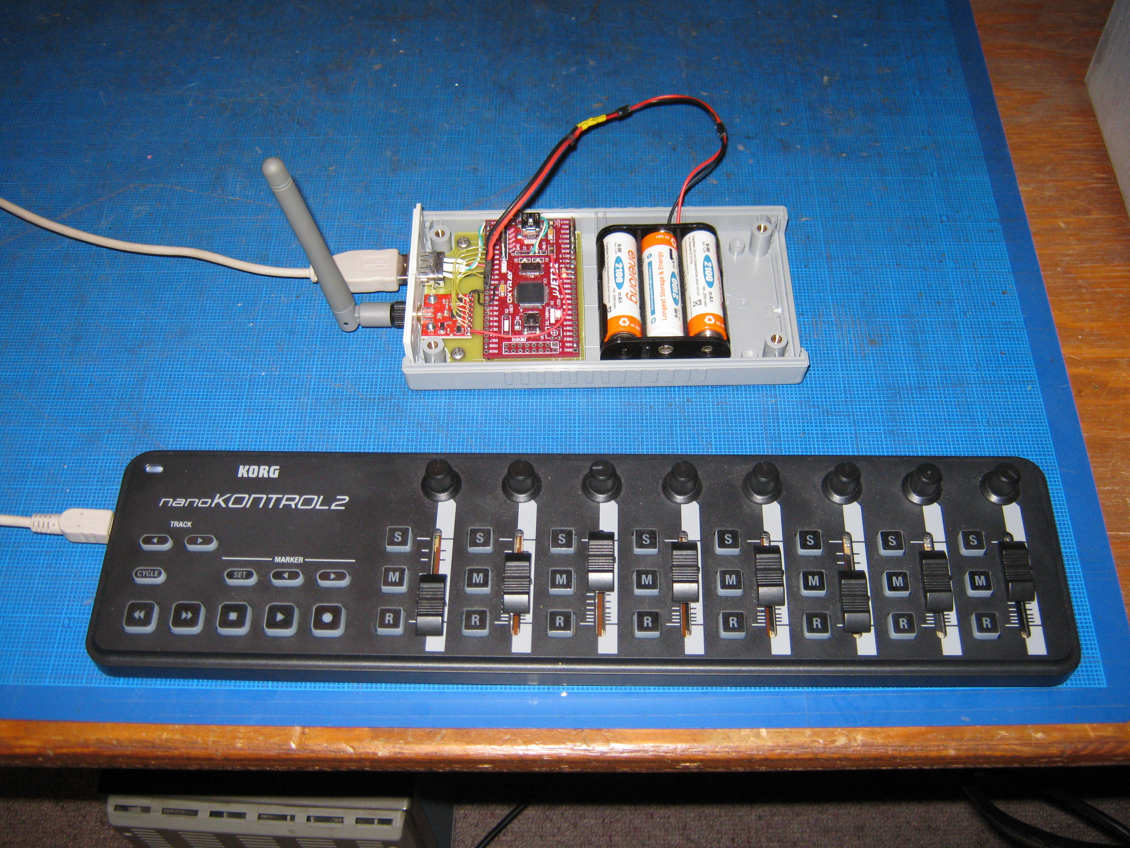
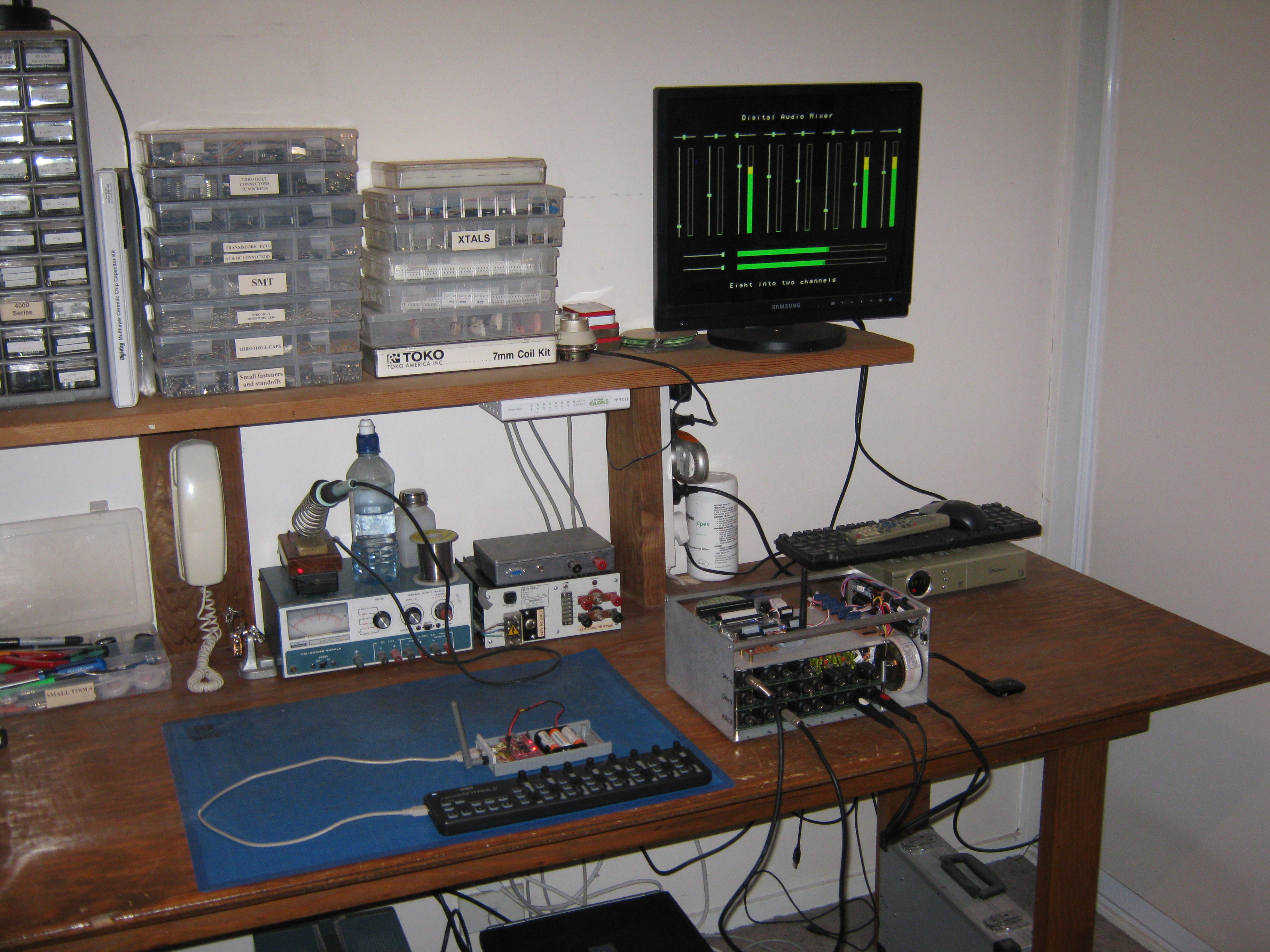
With the lid removed. An FR4 substrate was used to support the A type USB female, the wireless module and the uJET32 module with dsPIC processor. This assembly is secured using two M3 screws into the plastic case. Design and fabrication of the substrate and the plastic end plate took just over five hours work.
Power
Around 120mA at 5V is required to power the USB control surface, with something less than 80mA to drive the dsPIC and wireless. A safe bet is to budget around 200mA at 5V. So, to meet the four hour run time requirement, a battery capacity of 4 Watt Hours is needed. Some while ago I had been given a small pile of LiPo batteries including 3 in parallel 800mAh cells. So this pack is theoretically capable of 2400mAH at about 3V (minimum), so just over 7 Watt hours. Battery management is significantly eased by the use of single cell LiPos since charge balancing is not required.
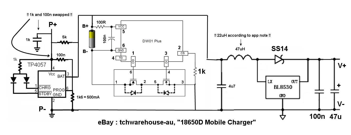
A small module has been acquired from eBay that connects directly to a LiPo cell and manages charge and discharge at 5V. Charge management is using a TP4057, battery protection is managed by a DW01+, and a BL8530 boost regulator converts cell voltage back to 5V.
With thanks to...
Comments and corrections always welcome.
Regards,
13 July 2013, New Zealand